- 您现在的位置:买卖IC网 > Sheet目录2007 > MAX11040GUU+T (Maxim Integrated Products)IC ADC 24BIT 4CH 38-TSSOP
MAX11040K/MAX11060
24-/16-Bit, 4-Channel, Simultaneous-Sampling,
Cascadable, Sigma-Delta ADCs
13
Maxim Integrated
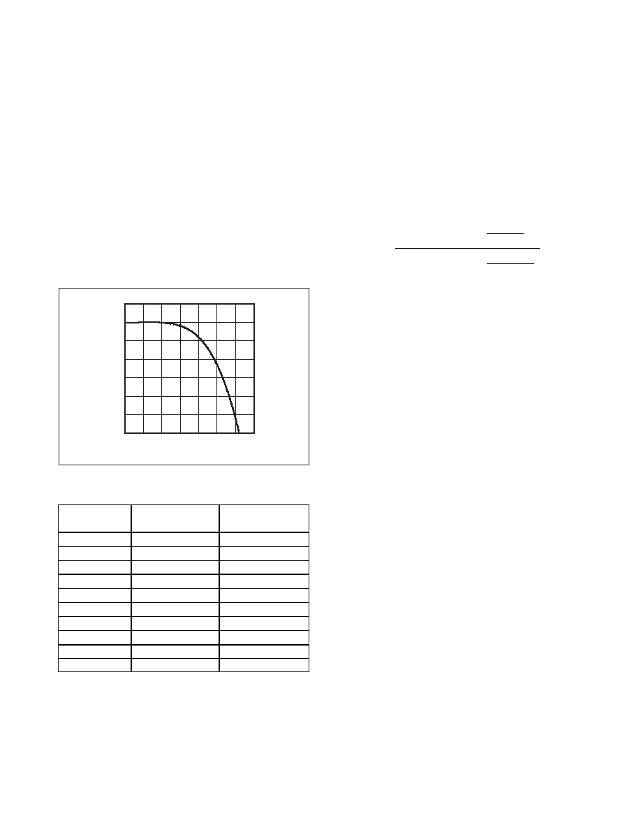
Digital Filter
The devices contain an on-chip digital lowpass filter
that processes the data stream from each modulator
and generates the high-resolution output data. The low-
pass filter frequency response is determined by the
programmable output data rate. At the nominal 16ksps
output data rate, the -3dB bandwidth of the filter is
3.4kHz. The passband flatness is better than ±0.1dB
from 0 to 1.74kHz. The notches are located at 5.75kHz
and 7.195kHz. These frequencies scale linearly with the
output data rate. See Figure 2 and Table 1 for the fre-
quency response at different data rates.
Since the transfer function of a digital filter is repeatable
and predictable, it is possible to correct for frequency-
dependent attenuation in downstream software. See
the
Compensating for the Rolloff of the Digital Filter in a
Typical FFT Analysis section. The transfer function is
defined by the following equation:
where:
Gain is the filter gain.
fAIN is the analog input frequency.
fSAMPLE is the programmed output data rate, nominally
16kHz.
fXINCLOCK is the clock frequency at XIN, nominally
24.576MHz.
FIR_Gain (fAIN) is the normalized gain of the FIR filter
with the following filter coefficients, as a function of the
analog input frequency fAIN. These coefficients are
applied at the output data rate:
+ 0.022
- 0.074
- 0.036
+ 0.312
+ 0.552
+ 0.312
- 0.036
- 0.074
+ 0.022
Gain f
f
AIN
SAMPLE
AIN
SAMPLE
()
sin
=
××
π
X
XINCLOCK
AIN
XINCLOCK
f
××
sin
π
×
()
3
_(
)
FIR Gain fAIN
Table 1. Bandwidth vs. Output Data Rate
OUTPUT DATA
RATE (ksps)
-3dB BANDWIDTH
(kHz)
-0.1dB BANDWIDTH
(kHz)
0.5
0.11
0.05
1
0.21
0.11
2
0.42
0.22
4
0.85
0.43
8
1.69
0.87
10
2.11
1.09
12
2.54
1.31
16
3.38
1.74
32
6.78
3.48
64
13.5
6.96
MAX11040K
fig02
fAIN/fSAMPLE
GAIN
(dB)
0.24
0.20
0.16
0.12
0.08
0.04
-5
-4
-3
-2
-1
0
1
-6
00.28
Figure 2. Digital Filter Response
发布紧急采购,3分钟左右您将得到回复。
相关PDF资料
MAX11046ECB+T
IC ADC 16BIT PAR 250KSPS 64TQFP
MAX11046ETN+T
ADC 16BIT SAMPLING 8CH 56-TQFN
MAX11049ECB+
IC ADC 16BIT PAR 250KSPS 64TQFP
MAX1104EUA+
IC CODEC 8BIT 8-UMAX
MAX11100EUB+
IC ADC 16BIT SRL 200KSPS 10UMAX
MAX11101EUB+
IC ADC 14BIT SRL 200KSPS 10UMAX
MAX11102AUB+
IC ADC 12BIT SPI/SRL 10UMAX-EP
MAX1111CPE+
IC ADC 8BIT LP 16-DIP
相关代理商/技术参数
MAX11040K
制造商:MAXIM 制造商全称:Maxim Integrated Products 功能描述:24-/16-Bit, 4-Channel, Simultaneous-Sampling, Cascadable, Sigma-Delta ADCs
MAX11040K_1111
制造商:MAXIM 制造商全称:Maxim Integrated Products 功能描述:24-/16-Bit, 4-Channel, Simultaneous-Sampling, Cascadable, Sigma-Delta ADCs
MAX11040K_12
制造商:MAXIM 制造商全称:Maxim Integrated Products 功能描述:MAX11040K Evaluation Kit/Daughterboard
MAX11040KDBEVKIT
制造商:MAXIM 制造商全称:Maxim Integrated Products 功能描述:MAX11040K Evaluation Kit/Daughterboard
MAX11040KDBEVKIT#
功能描述:数据转换 IC 开发工具 MAX5135/11040/11612 Eval Kit w/ FMC RoHS:否 制造商:Texas Instruments 产品:Demonstration Kits 类型:ADC 工具用于评估:ADS130E08 接口类型:SPI 工作电源电压:- 6 V to + 6 V
MAX11040KEVKIT
制造商:MAXIM 制造商全称:Maxim Integrated Products 功能描述:MAX11040K Evaluation Kit/Daughterboard
MAX11040KEVKIT#
功能描述:数据转换 IC 开发工具 MAX5135/11040/11612 Eval Kit w/ FMC RoHS:否 制造商:Texas Instruments 产品:Demonstration Kits 类型:ADC 工具用于评估:ADS130E08 接口类型:SPI 工作电源电压:- 6 V to + 6 V
MAX11040KGUU
制造商:MAXIM 制造商全称:Maxim Integrated Products 功能描述:24-/16-Bit, 4-Channel, Simultaneous-Sampling, Cascadable, Sigma-Delta ADCs